Git Product home page Git Product logo

jlc-plugin-for-kicad's Introduction

JLC PCB Plug-in for KiCad

JLC PCB Plug-in for KiCad

Sponsor

Features

  1. Generates gerber files in correct format for production
  2. Generates BOM file in correct format for production
  3. Generates Pick and Place file in correct format for assembly
  4. Generates IPC netlist file

Installation

Official Installation

Fabrication Toolkit is distributed with the official releases of KiCad 6+. Open the "Plugin and Content Manager" from the KiCad main menu and install the "Fabrication Toolkit" plugin from the selection list.

Manual installation

Download the latest release ZIP file. Open the "Plugin and Content Manager" from the KiCads main window and install the ZIP file via "Install from File".

Usage

Click on the Fabrication Toolkit Logo button on the top tool box inside KiCad pcb editor (pcbnew).

Ensure your board is syncronized before invoking this addon [F8].

The User_1 layer in internally defined as a V-Cuts layer, please avoid using it for anything else (unless disabled). (since v3.0.0).

Options

Options can be set in the dialog that appears when the plugin is invoked. They are saved in a file called fabrication-toolkit-options.json in the project directory so that they are remembered between invocations of the plugin.

Additional layers: Comma-separated list of additional layers to include in the gerber archive.
Set User.1 as V-Cut layer: Merge User.1 layer with the Edge-Cut layer in production.
Apply automatic translations: Apply known translation fixes for common components.
Apply automatic fill for all zones: Refill all zones before generation production files.
Exclude DNP components from BOM: Exclude components the had been set a DNP from th BOM.

① Include Component Part Number in Production Files

Add an 'LCSC Part #'* field with the LCSC component part number to the symbol's fields property.

Primary Fields*:

'LCSC Part #' 'JLCPCB Part #'

The fields will be query in the order denoted above.

Fallback Fields*:

'JLC Part' 'LCSC Part' 'LCSC' 'JLC' 'MPN' 'Mpn' 'mpn'

The fields will be query in the order denoted above.


② Ignore Footprint in Production Files

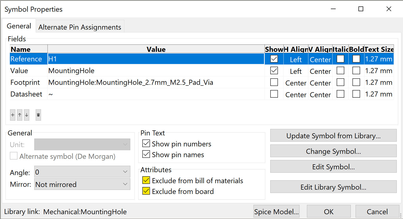
Select 'Exclude from board' or 'Exclude from BOM' in the symbol's attributes property in order to ignore the footprint from the relevant file.

Select 'Exclude from position files' or 'Exclude from BOM' in the footprint's fabrication attributes property in order to ignore the footprint from the relevant file.


③ Offset Component Rotation

The rotation of components in KiCad Footprints does not always match the orientation in the JLC library because KiCad and JLC PCB used different variation of the same standard. Most of the rotations may be corrected by the rotations.cf definitions. To the exception cases: add an 'JLCPCB Rotation Offset' field - with positive values indicating counter-clockwise orientation offset in degrees.

If the JLC preview shows a footprint like this, enter a rotation offset of -90 to rotate pin 1 to the lower right corner.

As the rotation offset is entered in the Schematic Editor, make sure to update your PCB with the changes made to the schematic before generating a new set of production files, otherwise your changes won't be reflected.

Primary Fields*:

'JLCPCB Rotation Offset'

The fields will be queried in the order denoted above.

Fallback Fields*:

'JlcRotOffset' 'JLCRotOffset'

The fields will be queried in the order denoted above.


④ Offset Component Position

The position of components in KiCad Footprints does not always match the orientation in the JLC library because KiCad and JLCPB used different variation of the same standard. To the exception cases: add an 'JLCPCB Position Offset' field with an comma separated x,y position offset to correct it.

Use following table to quickly find out to which coordinate enter the correction based on JLC arrows clicks - depending on footprint rotation in Kicad PCB Editor status bar:

Kicad footprint deg x y
0deg, Front right arrow up arrow
0deg, Back left arrow down arrow
180deg, Front left arrow down arrow
180deg, Back right arrow up arrow
90deg, Front or Back up arrow left arrow
-90deg, Front or Back down arrow right arrow

For custom angles it's best to place also a temporary straight symbol to perform alignment. Single arrow press in JLC is 0.0635mm (= 1/400in) shift.

As the position offset is entered in the Schematic Editor, make sure to update your PCB with the changes made to the schematic before generating a new set of production files, otherwise your changes won't be reflected.

Primary Fields*:

'JLCPCB Position Offset'

The fields will be queried in the order denoted above.

Fallback Fields*:

'JlcPosOffset' 'JLCPosOffset'

The fields will be queried in the order denoted above.

⑤ Override Component Layer

Some footprints may have their components defined on the opposite layer to there actual footprints. In these instances you can override mount side by using this field.

Values can be top, bottom, t or b.

Primary Fields*:

    | 'JLCPCB Layer Override' |
    | --- |

The fields will be queried in the order denoted above.

Fallback Fields*:

    | 'JlcLayerOverride' | 'JLCLayerOverride' |
    | --- | --- |

The fields will be queried in the order denoted above.

Author

Benny Megidish

jlc-plugin-for-kicad's People

Contributors

21km43 avatar alexisvl avatar antonxy avatar arxwtf avatar bennymeg avatar carlosgs avatar dzid26 avatar fisheiyy avatar harbaum avatar hildogjr avatar hrueger avatar kiu avatar llamasoft avatar lukas-lang avatar majorarkwolf avatar mengstr avatar miceuz avatar mojombo avatar msalau avatar obaterspok avatar pyjamasam avatar revk avatar thecolorman avatar tobsec avatar tylercrumpton avatar

Stargazers

 avatar  avatar  avatar  avatar  avatar  avatar  avatar  avatar  avatar  avatar  avatar  avatar  avatar  avatar  avatar  avatar  avatar  avatar  avatar  avatar  avatar  avatar  avatar  avatar  avatar  avatar  avatar  avatar  avatar  avatar  avatar  avatar  avatar  avatar  avatar  avatar  avatar  avatar  avatar  avatar  avatar  avatar  avatar  avatar  avatar  avatar  avatar  avatar  avatar  avatar  avatar  avatar  avatar  avatar  avatar  avatar  avatar  avatar  avatar  avatar  avatar  avatar  avatar  avatar  avatar  avatar  avatar  avatar  avatar  avatar  avatar  avatar  avatar  avatar  avatar  avatar  avatar  avatar  avatar  avatar  avatar  avatar  avatar  avatar  avatar  avatar  avatar  avatar  avatar  avatar  avatar  avatar  avatar  avatar  avatar  avatar  avatar  avatar  avatar  avatar

Watchers

 avatar  avatar  avatar  avatar  avatar  avatar  avatar  avatar  avatar  avatar  avatar

jlc-plugin-for-kicad's Issues

MPN not translating to the BOM

This may be an old issue that's reared up or something else - but I don't have the time to look.

I see from the code and the documentation that adding a string such as MPN, LCSC Part # and so on, allows us to add the LCSC part for the picker to automate. I've been relying on this for a while now and I'll be honest, I got complacent.

That was expensive! I just ordered a load of completed boards and they came back with a 5K6 resistor in place of the 60R ferrite bead. Not the end of the world as it's easily removed of course.

Entirely my fault for not checking (I was tired, that's my excuse) and JLC were really good about it.

But to the point, no matter what string I'm feeding the BOM the actual LCSC part number never gets spat out with the BOM and JLCPCB's scripting is trying to figure out what I meant from what's left. This is the first time I've encountered this but I was on Mac previously although I was using KiCAD 7.00.

I'll fix this manually for now (the drifting components and weird rotations I can do by hand) but the MPN "bug" is a real bind as it means I've got to do a separate BOM and make sure I send the right one! :)

Wrong components alignement on JLC

Dear

I notice that each time I upload the list to JLC, something wrogn appears regarding the components' alignemnt.
For isntance: here the diodes:

image

But it occurs also with Transistors and ICs. the rotation angle is always wrong.
OK JLC will corect by hands, but aside this, the files are getting wrong positioning I see.

EDIT: I opened also a topic here: https://forum.kicad.info/t/wrong-components-alignement-for-jlcpcb-not-clue-if-due-kicad-or-due-the-script/43772

Running the plugin creates a DRC error.

Using Kicad 7.0.5 on Windows and plugin version 2.2.0. It's a very strange behavior:

  1. In the PCB editor with all DRC's cleaned.
  2. Running the Fabrication Toolkit plugin to generate production files.
  3. Running the DRC verification now give an error, as if the plugin mutated something.

The issue is very consistent, and I could not see any change in the pcb file if I save it again.

Clear DRC
image

After running the plugin, a single error appears:
image
image

Please include instructions on how to run this plugin

After I installed this plugin, it took me some time to figure out how to use it to generated BOM and position files.

You may want to include it in the README.md file here. E.g. select plugin X from the menu Y in windows Z and this will generate the files in a subdirectory called fabrication under your kicad project directory. or something like that.

Anyway, great plugin. It will save me a lot of tedious mouse clicks.

positions.csv file does not update

About 2 months ago with version 2.0.0 (KiCad 6.0) and today with version 2.0 and 2.1 (KiCad 7.0) the positions file does not store the negative values only positive.
For example:
JLCPCB Rotation Offset : 90 or
JLCPCB Rotation Offset : -90 both have the same .csv file with positive numbers even checking with Note Pad. I have also tried all the Fallback Field examples with no luck. Thus as all values are positive JLCPCB will not make any corrections unless I edit in the '-' to the .csv.

*Edit: After doing another test JLC-Plugin-for-KiCad always outputs the Orientation from the footprint and not the rotation Offset.

As no one else has brought this up I'm sure I must be doing something wrong but can't see where.

image

404 Error While Updating JLC Library

When I attempt to update the local JLCPCB parts library by clicking the "Update library" button, I get an error popup saying "Failed to download the JLCPCB database CSV, error code 404". This has previously worked for me, and I can't think of anything that's changed on my end that could cause this. This is with Windows 10, KiCAD 6.0.9, and plugin version 1.2.0.

image

Happy to run any tests to figure out what's going on here.

Please check zones are filled

Hi,

When exporting fabrication outputs from KiCad it checks that all zones are filled and issue below warning if that is not the case:
image

It would be nice if this plugin could do the same. I just noticed because I had a board come back where I had moved a component without refilling the zone :(

-- john

JLCPCB Rotation Offset not working

I have tried JLCPCB Rotation Offset on a component that is the wrong way around, and the output is the same, whatever I do. Any ideas?

Same with JLCPCB Position Offset, no effect at all.

Please rename it JLCPCB ToolKit

Just for a better recognition, instead of to call it Fabrication Toolkit, pleas erename it into JLCPCB ToolKit.
All the other plugins (included PCBWay) are clearly identified.
Unfortunately this, it isn't.

Just the variable " self.name = "JLCPCB Toolkit""

thank you

BOM lines with similar values are merged even if they're completely different parts

I'm not sure I understand the purpose of #38 / #36. It results in some ill advised merges. I have a project with some 10µF 0805 capacitors and some 10µH 0805 inductors. The capacitors have a JLC part number specified, but the inductors don't (I'm skipping those parts). This plugin merges them together into a single BOM line:

"C104,C111,C142,C162,C172,C304,C311,C342,C362,C372,L101,L102,L301,L302",0805,14,10µ,C440198

Merging lines for totally different types of parts doesn't seem like a good idea. At very least, parts with different JLC/LCSC part number fields (including no field at all) probably shouldn't be merged...

Some files in gerber.zip are not recognized by JLCPCB.

When I uploaded this 4 layers gerber zip file to JLCPCB I am getting an error messages that some of the files were not recognized. Not sure what they are and why there are in the .zip file but would think naively that since this a JLC specific plugin, it should include only files JLC needs when it accepts a .zip file.

The main thing is that I don't know if this is normal or if somebody is missing from my order because of dropped files.

2023-05-15_20-53-12
gerber.zip

Plot options not setting "substract soldermask from silkscreen"

So far I manually created my gerber files for JLC based on this: https://support.jlcpcb.com/article/194-how-to-generate-gerber-and-drill-files-in-kicad-6

JLC recommends to enable "Substract soldermask from silkscreen" which I sometimes rely on due to "background art" bleeding into pads.

Is there a reason why you are not setting this?

https://github.com/bennymeg/JLC-Plugin-for-KiCad/blob/master/plugins/process.py#L32
plot_options.SetSubtractMaskFromSilk(False)

No way to override top/bottom

Some footprints may have a shadow part on the other side, such as the MX keys with hotswap option.
That is, the footprint itself may be on top but the wanted hot swap part is to be placed on bottom.

"DNP" items getting published in BOM

With #37 closed, this plugin shouldn't be including DNP items in either the BOM or the positions file.

However, with the latest 2.3.0 release (which reports itself as 2.2.0), items such as these are still included in the output:

image

JLC Rotation Offset different on back of PCB

I don't know if JLCPCB do something unusual here, but I have parts with an JLC Rotation offset which work correctly on the front of the PCB but wrong on the back. E.g. one that needed +90 on front needed -90 on back, and similarly one was 0 and 180. Does the rotation offset need adjusting when used on back of board?

As I am including the JLC Rotation Offset in my parts template it would help if I did not have to adjust this per side.

By the way, this is an awesome and useful plugin. Well done.

Feature Suggestion: allow custom field to be placed in 'footprint' column in BOM

Hi, and thanks for the great work!

Just a quick suggestion: as the official KiCad libraries include the library name, and are often too long (ex: 'Capacitor_SMD:C_1206_3216Metric' instead of '1206' as recommended by JLC), my usual practice is to append a custom field named 'JLCFP' for all symbols and fill in the short FP name. Would be wonderful if there is some sort of mechanism to replace the 'footprint' column contents with those in some custom field for all symbols.

Any advice appreciated!

Column headers/order

Probably my setup, but column headers are incorrect (not being renamed), and columns not in correct order!

I installed the Addin. refreshed addins, and clicked on the icon that appeared. Is there something else I should be doing?

No Dialog on M1 Mac

As far as I can tell, to use this plugin I'm supposed to click on the button in the top toolbar? A "Processing" box with a progress bar pops up for a second or two and then nothing. I wish I knew how to give more information than that. If I can assist in debugging in any way let me know

Add the ability to group bom

The BOM currently shows every part individually.

Please add the ability to group them by value.

Example

FROM:
"220nF","C1","C_0603_1608Metric"
"220nF","C2","C_0603_1608Metric"
"220nF","C3","C_0603_1608Metric"
"220nF","C4","C_0603_1608Metric"
"100nF","C18","C_0402_1005Metric"
"100nF","C54","C_0402_1005Metric"

TO:
"220nF","C1, C2, C3, C4","C_0603_1608Metric"
"100nF","C18, C54","C_0402_1005Metric"

Add an option to group identical BOMitems

Please add an option to group components in the generated bom file as it used to be in previous options. It reduce the mental noise and clarifies what components are of the same kind.

Old style (grouped)
https://github.com/zapta/ble_stepper_motor_analyzer/blob/main/hardware/JLCPCB/version_1_4_1/bom.csv

New style (non grouped)
https://github.com/zapta/ble_stepper_motor_analyzer/blob/main/hardware/JLCPCB/version_1_4_2/bom.csv

As a side note, just upgraded to KiCad 7.0 and notice that this plugin is now supported by the the plugin manager. This is a great improvement. Thanks.

Rotation in positions.csv file?

Sorry, this is a question, not a bug. Though might be a feature request... I searched but did not find an answer so asking here.

JLCPCB always has device rotations messed up (ok, maybe it's not their fault but often a part is not in the proper orientation in the positions.CSV file). Is there a way to specify this other than post editing the CSV file? I know JLCPCB will correct rotations but I'd rather not rely on a tech always doing the right thing.

[edit] Yes, I know I can change the rotations during ordering but I frequently reorder and would have to go through the same process every time - the less manual intervention the better.

Panelized PCB need unique designators when created with KiKit

When a pcb is panelized with KiKit it creates duplicate designators which causes JLC's SMT service to crash.

Example KiKit:
kikit panelize ^
--layout "grid; rows: 3; cols: 1; space: 2mm" ^
--tabs "fixed; width: 3mm; vcount: 2" ^
--cuts "mousebites; drill: 0.5mm; spacing: 1mm; offset: 0.2mm; prolong: 0.5mm" ^
--framing "railstb; width: 3mm; space: 2mm;" ^
--tooling "3hole; hoffset: 2.5mm; voffset: 1.5mm; size: 1.152mm" ^
--fiducials "3fid; hoffset: 5mm; voffset: 1.5mm; coppersize: 2mm; opening: 1mm;" ^
--text "simple; text: JLCJLCJLCJLC; anchor: mt; voffset: 1.5mm; hjustify: center; vjustify: center; height: 1mm; thickness: 0.2mm" ^
--post "millradius: 1mm" ^
source.kicad_pcb ^
/pnl/destination.kicad_pcb

Fix: Append duplicate designators with a unique ID in the bom and footprint file
thread_py.txt
.

Add information to output file names

Hello,
It would be great to have the output file names include some information (like InteractiveHTMLBom does for example):
the name of the project, the revision number, the date of revision, the date of creation, etc.
Thank you!

Seems not to be working on MacOs Ventura

The package loads ok via package manage and creates files for JLCPCB, however..

  • No option screen(s) open
  • The 'orientation' fixes from 'rotations.cf' are not applied.

Maybe the above are known problems?

MacOs Ventura (13.4.1 (a) )
Application: KiCad x86_64 on x86_64

Version: 7.0.6-0, release build

Libraries:
wxWidgets 3.2.2
FreeType 2.13.0
HarfBuzz 7.3.0
FontConfig 2.14.2
libcurl/7.88.1 (SecureTransport) LibreSSL/3.3.6 zlib/1.2.11 nghttp2/1.51.0

Platform: macOS Ventura Version 13.4.1 (a) (Build 22F770820b), 64 bit, Little endian, wxMac

Build Info:
Date: Jul 6 2023 22:01:07
wxWidgets: 3.2.2 (wchar_t,wx containers)
Boost: 1.82.0
OCC: 7.7.0
Curl: 7.77.0
ngspice: 38
Compiler: Clang 13.0.0 with C++ ABI 1002

Build settings:
KICAD_SPICE=ON

All output files into the ZIP

I noticed that the .ZIP file contains all the output files included the Bom.csv and the Positioning.csv, not only the Gerber files.
on JLCPCB is required that the ZIP contains only the Gerber and the other 2 ones are uploaded separately.
Uploading the ZIP with all the files in it (included the CSV) doesn't bring any benefit.

Rotation wrong on bottom of board for JLCPCB

The positions.csv is generated with Mid X, Mid Y, and Rotation "as viewed from top". This seems to be how KiCad works.

E.g. this is two 0603 resistors with rotation of 10 degrees.

Screenshot 2023-04-13 at 10 20 07

KiCad 3D view shows clearly.

a
b

As you can see the 10 degree rotations is "as viewed from top".

The positions.csv file looks like this... showing both as 10 degrees.

Designator,Mid X,Mid Y,Rotation,Layer
R1,3.0,5.0,10.0,top
R2,7.0,5.0,10.0,bottom

However, when loaded on JLCPCB the rotation on the bottom is wrong, e.g

Screenshot 2023-04-13 at 10 13 08

Screenshot 2023-04-13 at 10 13 18

Clearly JLC are expecting the rotation "as viewed from above the component".

The positions.csv file needed is

Designator,Mid X,Mid Y,Rotation,Layer
R1,3.0,5.0,10.0,top
R2,7.0,5.0,350.0,bottom

This works as expected.

Screenshot 2023-04-13 at 10 16 40

If a rotation offset is applied, it works as you would expect, just added to the rotation, and could be used as a -20 offset to "fix" the bottom layer in this case, but that only works if rotated 10 degrees. Rotate 20 and you need to change the JLCPCB Rotation Offset to -40 to fix it. This is why the offsets seemed not to work. It is not the offset that is wrong, it is that all rotations on the back of the board need to be inverted, so as to be "as viewed from above the component" and not "as viewed from top" in the way KiCad works.

I think if the JLCPCB Rotation Offset is applied first, when present, to correct for whatever orientation JLC have used for the part, but then all bottom side rotations are inverted, it will be consistent and avoid having to tweak the back of every board.

This was obviously not obvious as rotations 0, and 180 did not show the problem, and 90 or 270 only showed on polarised components. But even a simple 0603, with no need for any rotation offset, breaks if placed at 45 degrees, so I think this is a definite bug, and should be fixed even with the backwards compatibility issues it would cause.

Empty LCSC Part column in bom.cvs

The LCSC Part # column in my generated bom.cvs is empty. I have added the JLCPCB parts in Symbol Properties with field name MPN. I a lot of errors get printed to stderr when running the Fabrication Toolkit plugin .

Traceback (most recent call last):
  File "/home/goran/.local/share/kicad/6.0/3rdparty/plugins/com_github_bennymeg_JLC-Plugin-for-KiCad/plugin.py", line 46, in updateDisplay
    self.m_gaugeStatus.SetValue(status.data)

Im using:

Application: KiCad Schematic Editor

Version: 6.0.7-f9a2dced07116ubuntu22.04.1, release build

Libraries:
wxWidgets 3.0.5
libcurl/7.81.0 OpenSSL/3.0.2 zlib/1.2.11 brotli/1.0.9 zstd/1.4.8 libidn2/2.3.2 libpsl/0.21.0 (+libidn2/2.3.2) libssh/0.9.6/openssl/zlib nghttp2/1.43.0 librtmp/2.3 OpenLDAP/2.5.13

Platform: Linux 5.15.0-47-generic x86_64, 64 bit, Little endian, wxGTK, ubuntu, x11

Build Info:
Date: Jul 26 2022 19:32:47
wxWidgets: 3.0.5 (wchar_t,wx containers,compatible with 2.8) GTK+ 3.24
Boost: 1.74.0
OCC: 7.5.2
Curl: 7.84.0
ngspice: 36
Compiler: GCC 11.2.0 with C++ ABI 1016

Build settings:
KICAD_USE_OCC=ON
KICAD_SPICE=ON

and latest Fabrication Toolkit from Plugin and Content Manager.

Screenshot from 2022-09-25 19-32-45
Screenshot from 2022-09-25 19-34-34
kicad-output.txt

Part numbers ignored in KiCAD 7.0.2

I've tried using LCSC Part #, LCSC, and MPN as fields, but the plugin appears to be ignoring these and leaving the part number blank in the output bom.csv.

I'm using KiCAD 7.0.2

Add support for "Do Not Populate"

In Version 7, there is now a field to indiate a component is "Do Not Populate".
It would be great if this plugin would use this to leave it out of the BOM or perhaps add it but with DNP as value but remove LCSC.

Clears `production` of any files, no question asked

I have (had) a habit to save the files regarding production runs into a folder called ehh... production. Containing subdirs per hardware version/revision that was/is to be produced. This includes: schematics, gerber- and position files, parts quotes, 3D/CNC files etc.

By clicking the 'Fabrication Toolkit' icon in my PCB editor, the plugin is so 'kind' to throw all files contained in this directory away for me, with no questions asked. I get the fact that this is open source software without any guarantee and provided as-is.... but still this behavior seems somewhat 'rude' to me. Can the plugin be made to ask for a destination folder or at least ask for confirmation before deleting a whole bunch of files...? Many 🙏🏻

JLCPCB Fabrication Toolkit: how to save in the project dir?

It's not an issue but a request

I posted it here: https://forum.kicad.info/t/jlcpcb-fabrication-toolkit-how-to-save-in-the-project-dir/36684/3 they suggested me to post here

I re-write it here:
I discovered the Fabrication Toolkit JLCPCB.

Excellent! Thank you so much to all programed this tool. It makes the life way easier.

I need a help from you now.

using that tool, it saves the output to a subfolder of the TEMP folder.
Instead of manually copy and paste the content into the project folder, is it possible to set it up to save it automatically into the project folder instead of the Temp?

Thank you a zillion for this tool and for the help you will give me.

AttributeError: 'PCB_PLOT_PARAMS' object has no attribute 'SetExcludeEdgeLayer'

I get this error in the terminal when executing it from the toolbar in pcbnew. The "Processing" dialog just gets "stuck".

Exception in thread Thread-1:
Traceback (most recent call last):
  File "/usr/lib/python3.10/threading.py", line 1016, in _bootstrap_inner
    self.run()
  File "/home/.../.local/share/kicad/6.99/3rdparty/plugins/com_github_bennymeg_JLC-Plugin-for-KiCad/thread.py", line 31, in run
    self.process_manager.generate_gerber(temp_dir)
  File "/home/.../.local/share/kicad/6.99/3rdparty/plugins/com_github_bennymeg_JLC-Plugin-for-KiCad/process.py", line 30, in generate_gerber
    plot_options.SetExcludeEdgeLayer(True)
AttributeError: 'PCB_PLOT_PARAMS' object has no attribute 'SetExcludeEdgeLayer

Plugin version: 1.1.1

Kicad version info:

Application: KiCad PCB Editor

Version: (6.99.0-3101-g667a54ad86), release build

Libraries:
	wxWidgets 3.2
	FreeType 2.12.1
	HarfBuzz 5.1.0
	FontConfig 2.14.0
	libcurl/7.84.0 OpenSSL/1.1.1q zlib/1.2.12 brotli/1.0.9 zstd/1.5.2 libidn2/2.3.3 libpsl/0.21.1 (+libidn2/2.3.0) libssh2/1.10.0 nghttp2/1.48.0

Platform: Linux 5.19.4-arch1-1 x86_64, 64 bit, Little endian, wxGTK, i3, x11

Build Info:
	Date: Aug 28 2022 20:16:35
	wxWidgets: 3.2.0 (wchar_t,wx containers) GTK+ 3.24
	Boost: 1.79.0
	OCC: 7.5.3
	Curl: 7.84.0
	ngspice: 37
	Compiler: GCC 12.2.0 with C++ ABI 1017

Build settings:
	KICAD_USE_EGL=ON
	KICAD_SPICE=ON

Fabrication fails when running from unsaved PCB

https://github.com/bennymeg/JLC-Plugin-for-KiCad/blob/4a59fb0672f798ef9646803f915b3ed3bf244e96/plugins/thread.py#L26-L27

I ran into this issue when I was trying to export a panelized board for production. KiKit's panelization utility (https://yaqwsx.github.io/KiKit/v1.3/panelization/gui/) "is designed to be run in a standalone instance of Pcbnew (not executed from a project) as the generated panel replaces the currently open board". As a result, I was attempting to fabricate an unsaved PCB that didn't belong to a project. It looks like the plugin still tried to do something but the end result was it attempting to open file:///production/ which didn't exist and the output files were nowhere to be found. 😅

Does not work for more than 6 layers

When checking the gerber files, only a maximum of 6 layers get pushed to the gerber file. A project I was working on uses 10 copper layers but not all of them get included in the gerber file.

Pick and place data is broken when uploading to JLCPCB

When creating an SMD service order with JLCPCB, the placement data is not interpreted well by JLCPCB and all the parts are placed outside the board.

To preproduce:
Create a JLCPCB SMD service order with the files in the attached production.zip which were generated by Kicad 6.0.7 and this plugin. When you get to the 2D/3D board view, all the components are placed away from the board as shown here https://i.imgur.com/CCbHAmx.png
production.zip

Sanity check:
Do the same with the files in the attached easy_eda_fab.zip. These files were exported from an easy eda design and do work.
easy_eda_fab.zip

I believe that this is a recent change in JLCPCB and not specific to this plugin, but posting here such that it can be adapted to generate files compatibles with JLCPCB.

Use a predefined rotation file

JLCPCB and Kicad use a different patter to quadrant position of footprints pin-1 to mark the 0 degree angle. That is several threads about this discussion on forum.

In practical away there is a standard rotation for most of the footprints, in the past I used/update a old package about. It use this definition file that we cold merge to this project:
https://github.com/hildogjr/kicad_jlcpcba/blob/master/rotations.cf

All the footprints that match with regular expression defined at the file follow the specified rotation.

Semantic error

MPN mans Manufacturer Part Number.

This is a different meaning to distributor part numbers, such as LCSC Part # (recently encouraged by JLC to be renamed to JLCPCB Part #).

However, in your plugin, about which I learned after watching this MCH video seems to be positioned as the de-facto predominant interface for JLC for Kicad 6, I would recommend best practice approach, ie.

  • Do not call distributor part numbers 'MPN'
  • Realise that these fields represent different information and may both be present
  • In a situation in which more than one field is present, clarify in documentation which fields will be used in which order.

Given that so many people come to KiCad as a first EDA experience I believe it is extra important to get this right.

As I have not yet upgraded to KiCad 6.x from KiCad 5.1.x (mostly due to the huge amount of custom tooling in use) I regret that I do not have a test environment or familiarity to provide a pull request myself.

Add support for kicad 6 text variables

For export purposes, it is desirable to have the output production folder name be customizable (rather than just 'production'), akin to the PCB Editor Plot dialog (I have attached an example schema we use in our projects).
example_plot_variables

This would allow users to name the production folder in an algorithmic way, including project names, versions, etc.

Feature: Warning if part number is not given, while included in BOM

I have ordered a PCB, then later realizing a part had missing jlcpcb part numer, and jlcpcb picked the wrong component automatically.
I propose to display a warning dialogue listing parts which is missing the part number and "Exclude from bill of materials" is not checked.
There is a possible edge case where a part is supposed to be part of BOM, but part number not included. In such cases, i would rather be explicit about it, adding the part numer value "-" for example.

Part to be included in BOM but without part number proposal:

Reference Value
LCSC -

Part to be included in BOM but missing part number warning dialogue:

Warning
The following components is part of BOM but missing JLCPCB part number: [U2, R10]

in method 'BOARD_DESIGN_SETTINGS_m_SolderMaskMargin_set', argument 2 of type 'int'

This was working until I replaced a component with one that is an LCSC part, and now I get this error message when I try to run it. I tried deleting the footprint for the new part from the board, and I even tried deleting the part itself from the schematic to see if it was something specific to that part, but even without it I get this message.

I haven't changed any solder mask setting from the default. I've looked around for a solder mask setting which is not a number, but I haven't found anything. Is there any place that might have more details on what is wrong?

Recommend Projects

  • React photo React

    A declarative, efficient, and flexible JavaScript library for building user interfaces.

  • Vue.js photo Vue.js

    🖖 Vue.js is a progressive, incrementally-adoptable JavaScript framework for building UI on the web.

  • Typescript photo Typescript

    TypeScript is a superset of JavaScript that compiles to clean JavaScript output.

  • TensorFlow photo TensorFlow

    An Open Source Machine Learning Framework for Everyone

  • Django photo Django

    The Web framework for perfectionists with deadlines.

  • D3 photo D3

    Bring data to life with SVG, Canvas and HTML. 📊📈🎉

Recommend Topics

  • javascript

    JavaScript (JS) is a lightweight interpreted programming language with first-class functions.

  • web

    Some thing interesting about web. New door for the world.

  • server

    A server is a program made to process requests and deliver data to clients.

  • Machine learning

    Machine learning is a way of modeling and interpreting data that allows a piece of software to respond intelligently.

  • Game

    Some thing interesting about game, make everyone happy.

Recommend Org

  • Facebook photo Facebook

    We are working to build community through open source technology. NB: members must have two-factor auth.

  • Microsoft photo Microsoft

    Open source projects and samples from Microsoft.

  • Google photo Google

    Google ❤️ Open Source for everyone.

  • D3 photo D3

    Data-Driven Documents codes.