Package generated by Jinwoo Kim, PhD student in GTCAD laboratory, Georgia Institue of Technology.
Questions? email: [email protected]
This work was supported by the DARPA CHIPS program.
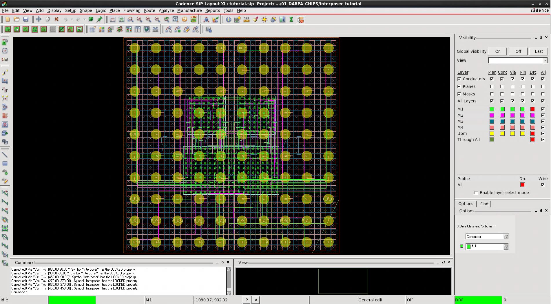
This standalone package shows an example of how to use Cadence SiP Layout to perform the basic chiplet PnR(place & route) on the interposer. The generated project file is *.sip, which contains all details of the design. All the files you need to generate the design are included in this directory. The detail of the interposer technology is as below:
- 65nm silicon interposer
- metal layer #: 4
- metal w/s: 0.4um/0.4um
- u-bump diameter/pitch: 20um/40um
- C4 bump diameter/pitch: 90um/180um
You will also need access to the following tools:
- Cadence SiP Layout XL 17.2
- Cadence PCB Automatic Router
- REAME.txt : this file
- ./design/env : source file to run Cadence SiP Layout XL 17.2
- ./design/:run_sip : c-shell script to invoke Cadence SiP Layout XL 17.2, import techfile, and perform chiplet placement
- ./die_data/T1_data.txt : the information of the chiplet T1 including origin and u-bump information
- ./die_data/T2_data.txt : the information of the chiplet T2 including origin and u-bump information
- ./die_data/U_data.txt : the information of the chiplet U including origin and u-bump information
- ./die_data/INTERPOSER_data.txt : the information of the interposer including origin and C4 bump information
- ./die_data/chiplet_list.txt : the list of chiplets in this design
- ./die_data/INTERPOSER_vdd_position.txt : the position of VDD C4 bumps on the interposer
- ./die_data/INTERPOSER_vss_position.txt : the position of VSS C4 bumps on the interposer
- ./result/ : the result directory to save the design reports
- ./script/bash_script/make_sip_script.sh : bash script to generate the SiP script for importing techfile, the chiplet placement, and the grid setting
- ./script/bash_script/make_techfile.sh : bash script to generate the techfile of the design
- ./script/bash_script/make_vdd_script.sh : bash script to generate the SiP script for PDN, VDD mesh
- ./script/bash_script/make_vss_script.sh : bash script to generate the SiP script for PDN, VSS mesh
- ./via_data/* : via definition files
-
Run the bash script from this home directory:
-
bash ./script/bash_script/make_techfile.sh
- This will generate the techfile in ./script/techfile directory.
-
bash ./script/bash_script/make_sip_script.sh
- This will generate SiP scripts for importing the techfile, the chiplet placement, and the grid setting.
-
bash ./script/bash_script/make_vdd_script.sh
-
bash ./script/bash_script/make_vss_script.sh
-
bash ./script/bash_script/make_vdd_via.sh
-
bash ./script/bash_script/make_vss_line.sh
- These will generate SiP scripts for PDN generation, VDD and VSS (please run the script for VDD first).
-
-
Copy all via definition files into ./design directory.
- cp ./via_data/* ./design/
-
Run the sciprt from ./design directory.
- source :run_sip
- This will execute Cadence SiP Layout XL, import the techfile, modify the grid setting, import the information of chiplets and run the placement.
- source :run_sip
-
Change 'Active Class and Subclass' from 'Substarte Geometry' to 'Conductor' in 'Options' tab.
-
Create fanouts on the interposer.
- Route -> Create Fanout
- In 'Options' tab,
- Start layer : M4
- End layer : Ubm
- Via : TSV
- Via Direction: Via in Pad
- Click any C4 bump on the interposer.
- Type 'done' in the command window.
-
Type the following commands in the command window to generate PDN mesh.
- replay ../script/PDN_script/add_vdd_mesh.scr
- replay ../script/PDN_script/add_vss_mesh.scr
-
Type the following commands in the command window to add power connections from the interposer to PDN.
- replay ../script/PDN_script/add_vdd_via.scr
- replay ../script/PDN_script/add_vss_line.scr
-
Run Automatic Router.
- Route -> Router -> Route Automatic
-
Setup Automatic Router options.
- 'Router Setup' tab.
- 'Options' section
- Check 'Limit wraparounds'
- Check 'Protect existing routes'
- Metal layer selection (check Protect as well).
- M1/M2/M3/M4
- 'Options' section
- 'Selections' tab.
- Objects to route:
- All but selected
- Move the following objects into 'Selected Objects'.
- VDD
- VSS
- Objects to route:
- 'Router Setup' tab.
-
Click 'Route' to run Automatic Router and click 'Close' after routing.
- Automatic Router performs the signal routing in Manhattan routing.
-
VDD routing.
- Open 'Cross Section Editor'.
- Setup -> Cross-section
- Change layer name 'M3' to 'VDD'.
- Change layer type from 'Conductor' to 'Plane'.
- Click 'OK'.
- Run Automatic Router.
- 'Selections' tab.
- Objects to route: All selected
- Move 'VDD' into 'Selected Objects'.
- Click 'Route' to run Automatic Router and click 'Close' after routing.
- 'Selections' tab.
- Open 'Cross Section Editor'.
- Setup -> Cross-section
- Change layer name 'VDD' to 'M3'.
- Change layer type from 'Plane' to 'Conductor'.
- Click 'OK'.
- Open 'Cross Section Editor'.
-
VSS routing.
- Open 'Cross Section Editor'.
- setup -> Cross-section
- Change layer name 'M4' to 'VSS'.
- Change layer type from 'Conductor' to 'Plane'.
- Click 'OK'.
- Run Automatic Router.
- 'Selections' tab.
- Objects to route: All selected
- Move 'VSS' into 'Selected Objects'.
- Click 'Route' to run Automatic Router and click 'Close' after routing.
- 'Selections' tab.
- Open 'Cross Section Editor'.
- Setup -> Cross-section
- Change layer name 'VSS' to 'M4'.
- Change layer type from 'Plane' to 'Conductor'.
- Click 'OK'.
- Open 'Cross Section Editor'.
-
Save design.
-
Generate and save design reports into ./result/ directory.
- Wirelength report.
- Reports -> Quick Reports -> Conductor Length by Pin Paire Report
- Via usage report.
- Reports -> Quick Reports -> Via List by Net Report
- DRC report.
- Reports -> Quick Reports -> Design Rules Check (DRC) Report
- Wirelength report.
